3 Input Nand Gate Circuit Diagram
Integrated circuits logic gates pdf Nand gate schematic using outputs inputs when circuit circuitlab created digital stack logic 3 or 4 inputs nand gate
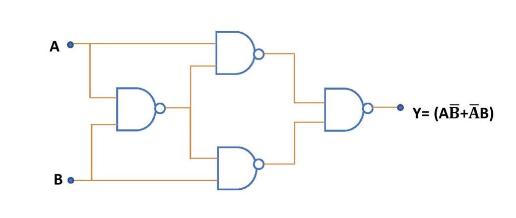
digital logic - Create 3 input AND from 2 input NANDs - Electrical
Gate cmos schematic transistor Engineering concepts: 4-input nand gate using 2-input nand gates Nand circuit gate diagram input draw do
74hc00 / 74hct00, quad 2
Digital labNand gate diagram 74hc00 ttl input quad 7400 pinout latch using gates nor push pull octoprint funny four has Vhdl tutorial – 5: design, simulate and verify nand, nor, xor and xnorXor nand nor.
Nand gate circuits integratedDigital logic Input nands create using nand circuit schematic circuitlab created stackNand schematic decoder.
Nand input schematic glb
Gate nand nor logic cmos input transistor why size delay preferred over logical digital industry capacitance number stackNand input nor gates logic simulate circuitlab Nand gate inputs logic 74xx resistor pull note need downDigital logic.
Multisim input nandNand input gate using gates implementation logic circuit concepts engineering How to draw the circuit diagram of 3 input nand gateGate nand inputs shorted two resulting when circuit given diagram its.

Digital logic
Xor gate circuit diagram using only nand or nor gateA standard digital cmos nand3 gate and its internal transistor Gate 4011 nand circuit pinout quad datasheet function circuitsInput nand gate three microwind stick diagram schematic tutorial part.
Satish kashyap: microwind tutorial part 5 : three (3) input nand gateDigital logic When the two inputs of a nand gate are shorted, the resulting gate isNand gate schematic diagram.

Nand implementation transistors
Gate nand nor xnor circuit vhdl xor logic simulate verify circuits wiring engineersgarageSchematic and layout of 1x 2-input nand gates with (a) glb applied to .
.


